Pages

Image and video hosting by TinyPic

cari duit gampang...cobain deh

Power Supply negatif dari tegangan positif


Op amps sangat berguna. Tapi salah satu kelemahan utama mereka adalah kebutuhan pasokan ganda. Ini serius membatasi aplikasi mereka dalam bidang di mana pasokan ganda tidak terjangkau atau tidak praktis.
Sirkuit ini memecahkan masalah sampai batas tertentu. Ini memberikan tegangan negatif dari catu positif tunggal. Ini tegangan negatif bersama dengan pasokan positif dapat digunakan untuk menyalakan opamps dan sirkuit lain yang membutuhkan pasokan ganda.


Operasi sirkuit dapat dijelaskan sebagai berikut:
IC 555 beroperasi sebagai multivibrator astabil dengan frekuensi sekitar 1kHz. Gelombang persegi ini diperoleh pada 3 pin dari IC. Ketika output adalah positif, biaya kapasitor 22uF melalui dioda D1. Bila output pada pin 3 adalah tanah, pembuangan 22uF melalui dioda D2 dan biaya kapasitor 100uF dibebankan. Output diambil melintasi kapasitor 100uF seperti yang ditunjukkan pada gambar.


Kerugian dari rangkaian ini adalah miskin tegangan peraturan dan batas saat ini. Maks. saat ini yang dapat ditarik dari rangkaian ini adalah sekitar 40mA. Jika Anda menarik lebih saat ini, peraturan tersebut akan hilang.
Juga tegangan output negatif akan menjadi sedikit kurang dari suplai positif karena tetes dioda. Sebagai contoh jika tegangan 9V maka tegangan output akan sekitar 7,5 V.

switching Power Supply tunggal


        Salah satu fitur utama dari sirkuit diatur listrik yang disajikan adalah bahwa meskipun tetap tegangan regulator LM7805 digunakan di sirkuit, tegangan output adalah variabel. Hal ini dicapai dengan menghubungkan potensiometer antara terminal umum dari IC regulator dan tanah. Untuk setiap kenaikan 100-ohm nilai di-sirkuit perlawanan potensiometer VR1, kenaikan tegangan output sebesar 1 volt. Dengan demikian, output bervariasi dari 3.7V ke 8.7V (dengan mempertimbangkan penurunan 1,3 volt di seluruh dioda D1 dan D2).


Fitur lain yang penting dari pasokan adalah bahwa ia mati sendiri ketika tidak ada beban yang terhubung di terminal output. Hal ini dicapai dengan bantuan transistor T1 dan T2, dioda D1 dan D2, dan kapasitor C2. Ketika beban terhubung di drop, output potensial di dioda D1 dan D2 (sekitar 1.3v) sudah cukup untuk transistor T2 dan T1 untuk melakukan. Akibatnya, relay akan energi dan tetap dalam keadaan itu selama beban masih terhubung. Pada saat yang sama, kapasitor C2 dapat diisi ulang untuk sekitar 7-8 potensi volt melalui transistor T2. Tapi ketika beban dilepas, transistor T2 terputus. Namun, kapasitor C2 akan tetap dikenakan biaya dan mulai pemakaian melalui basis transistor T1. Setelah beberapa waktu (yang pada dasarnya ditentukan oleh nilai C2), relay RL1 adalah de-energized, yang akan mematikan listrik untuk masukan utama transformator X1. Untuk melanjutkan kekuasaan lagi, saklar S1 harus ditekan sesaat. Tinggi nilai kapasitor C2, lebih akan penundaan mematikan catu daya pada pemutusan beban, dan sebaliknya.


      Meskipun dalam prototipe sebuah transformator dengan tegangan sekunder 12V-0V, 250mA digunakan, namun demikian dapat diubah sesuai kebutuhan pengguna (hingga maksimum 30V dan 1-ampere nilai sekarang.). Untuk menarik lebih dari 300mA saat ini, IC regulator harus dilengkapi dengan heat sink kecil selama isolator mika. Ketika tegangan sekunder transformator meningkat melampaui 12 volt (RMS), potensiometer VR1 harus redimensioned. Juga, voltase estafet harus ditentukan ulang

Regulator penurun tegangan rendah linier


Rangkaian adalah MOSFET berdasarkan regulator tegangan linier dengan penurunan tegangan terendah 60 mV pada 1 ampere. Setetes milivolt lebih sedikit mungkin dengan MOSFET lebih baik memiliki lebih rendah RDS (on) perlawanan. Rangkaian pada Gambar. 1 menggunakan 15V-0-15V sekunder dari transformator step down dan mempekerjakan sebuah MOSFET saluran-n IRF 540 untuk mendapatkan output 12V DC diatur dari input, yang dapat serendah 12.06V. Drive gerbang tegangan yang diperlukan untuk MOSFET dihasilkan menggunakan sirkuit Doubler tegangan yang terdiri dari dioda D1 dan D2 dan kapasitor C1 dan C4. Untuk mengaktifkan MOSFET sepenuhnya pada, terminal gerbang akan menjadi sekitar 10V di atas terminal sumber yang terhubung ke output di sini. The Doubler tegangan feed tegangan ini ke pintu gerbang melalui resistor R1. Shunt regulator adjustable TL431 (IC2) digunakan di sini sebagai penguat kesalahan, dan secara dinamis menyesuaikan tegangan gerbang untuk mempertahankan regulasi pada output. Dengan heatsink yang memadai untuk MOSFET, sirkuit dapat memberikan hingga keluaran 3A di drop minimal sedikit lebih tinggi tegangan. Trimpot VR1 di sirkuit yang digunakan untuk penyesuaian halus dari tegangan output. Kombinasi R2 C5 dan resistor kapasitor menyediakan kesalahan-penguat kompensasi. Rangkaian ini dilengkapi dengan perlindungan sirkuit pendek gagak-bar untuk menjaga komponen terhadap over-stress selama pendek disengaja pada output. Perlindungan ini gagak-bar akan bekerja sebagai berikut: Di bawah kondisi kerja normal, tegangan kapasitor C3 akan 6.3V dan dioda D5 akan dalam keadaan off karena akan reverse-bias dengan tegangan output dari 12V. Namun, selama keluaran arus pendek kondisi, output sesaat akan turun, menyebabkan D5 untuk melakukan dan OPTO-triac MOC3011 (IC1) akan mendapatkan dipicu, merobohkan tegangan gerbang ke tanah, dan dengan demikian membatasi output saat ini. Sirkuit akan tetap terkunci dalam keadaan ini, dan tegangan input harus dimatikan untuk mengatur ulang sirkuit. Sirkuit yang ditunjukkan pada Gambar. 2 berikut skema serupa. Hal ini dapat digunakan ketika regulator harus bekerja dari rel DC di tempat 15V-0-15V AC pasokan. Tegangan gerbang sini dihasilkan dengan menggunakan rangkaian LM555 biaya pompa sebagai berikut: Ketika 555 output rendah, C2 kapasitor akan mendapatkan diisi melalui dioda D1 dengan tegangan input. Pada setengah siklus berikutnya, ketika output 555 pergi tinggi, C3 kapasitor akan bisa dikenakan biaya untuk hampir dua kali lipat tegangan input. Seluruh rangkaian bekerja dengan cara yang sama sebagai rangkaian dari Gambar. 1. Sirkuit ini di atas akan membantu mengurangi daya-rugi dengan memungkinkan untuk menjaga rentang tegangan masukan lebih rendah untuk regulator selama desain awal atau bahkan di sirkuit yang ada. Ini akan menjaga output diatur dengan tegangan input relatif rendah dibandingkan dengan regulator konvensional. Jatuh tegangan minimal dapat lebih dikurangi dengan menggunakan RDS rendah (pada) MOSFET atau paralelisasi mereka.

Stabiliser tegangan listrik


 tegangan cut-out akan menghemat peralatan mahal Anda listrik dan elektronik dari efek yang merugikan dari tegangan listrik sangat tinggi dan sangat rendah. Sirkuit ini memiliki ulang otomatis dan menggunakan komponen yang mudah tersedia. Itu membuat penggunaan pembanding tersedia di dalam IC 555 timer. Pasokan disadap dari berbagai sudut sirkuit power supply untuk relay dan kontrol operasi rangkaian untuk mencapai reliabilitas. Sirkuit ini menggunakan komparator 2 untuk kontrol sedangkan pembanding 1 output (terhubung ke pin ulang R) dijaga tetap rendah dengan korslet pin 5 dan 6 dari 555 IC. Pin masukan positif dari pembanding 2 adalah di 1/3rd tegangan Vcc. Jadi selama pin masukan negatif 2 kurang positif dari Vcc 1/3, komparator 2 output tinggi dan internal flip-flop diatur, yaitu yang output Q (pin 3) cukup tinggi. Pada saat yang sama pin 7 adalah dalam keadaan impedansi tinggi dan LED terhubung ke pin 7 menjadi off. Output (di pin 3) membalikkan (pergi rendah) ketika pin 2 diambil lebih positif dari 1/3 Vcc. Pada saat yang sama pin 7 pergi rendah (sebagai * ouptput Q dari flip-flop internal yang tinggi) dan LED terhubung ke pin 7 menyala. Kedua timer (IC1 dan IC2) dikonfigurasi untuk berfungsi dalam cara yang sama. Preset VR1 disesuaikan untuk di bawah tegangan (katakanlah 160 volt) cut-out dengan mengamati bahwa LED1 hanya menyala ketika tegangan listrik sedikit lebih besar dari 160V AC. Pada pengaturan ini output pada pin 3 dari IC1 rendah dan transistor T1 adalah cut-off negara. Sebagai hasil RESET * pin 4 dari IC2 diadakan tinggi karena terhubung ke Vcc melalui 100 kilo-ohm resistor R4. Preset VR2 disesuaikan dengan tegangan lebih (katakanlah 270V AC) cut-out dengan mengamati bahwa LED2 hanya memadamkan ketika tegangan listrik sedikit kurang dari 270V AC. Dengan RESET * pin 4 dari IC2 tinggi, output pin 3 juga tinggi. Sebagai hasil transistor T2 melakukan dan memberikan energi RL1 relay, menghubungkan beban ke catu daya melalui N / O-nya kontak. Ini adalah situasi selama tegangan listrik lebih besar dari 160V AC tetapi kurang dari 270V AC. Ketika listrik tegangan melampaui AC 270V, hal itu menyebabkan output pin 3 dari IC2 pergi rendah dan transistor cut-off T2 dan de-estafet memberi energi RL1, meskipun RESET * pin 4 masih tinggi. Ketika listrik tegangan menurun di bawah 160V AC, IC1s pin 3 menjadi high dan LED1 dipadamkan. Output tinggi di pin 3 hasil dalam konduksi dari transistor T1. Sebagai seorang kolektor hasil dari transistor T1 seperti juga RESET * pin 4 dari IC2 ditarik rendah. Dengan demikian output dari IC2 pergi rendah dan T2 transistor tidak melakukan. Sebagai akibatnya, relay RL1 adalah de-energized, yang menyebabkan beban akan terputus dari pasokan. Ketika listrik tegangan lagi melampaui 160V AC (tetapi kurang dari 270V AC) relay lagi memberikan energi untuk menghubungkan beban ke catu daya

Stabiliser tegangan pada power suara

 Variasi tegangan dan pemadaman listrik mempengaruhi berbagai alat tersebut seperti TV, VCR, sistem musik dan lemari es. Rangkaian sederhana akan melindungi peralatan mahal dari tinggi serta tegangan rendah dan tegangan surge (ketika kekuatan resume). Hal ini juga memberikan sebuah lagu merdu ketika daya listrik kembali. Ketika listrik tegangan normal, tegangan DC pada katoda dari dioda zener D4 kurang maka 5.6V. Sebagai hasil transistor T1 adalah dalam keadaan off. Tegangan DC pada katoda dari dioda zener D5 lebih besar dari 5.6V dan sebagai transistor T2 hasilnya adalah dalam pada negara. Akibatnya, relay RL1 akan energi, yang ditandai dengan menyalakan LED hijau. Dalam kondisi tegangan listrik tinggi, transistor T1 beralih ke pada negara karena tegangan pada katoda dari dioda zener D4 menjadi lebih besar dari 5.6V. Akibatnya, switch transistor T2 untuk keadaan off, sehingga relay untuk de-memberi energi bawah kondisi tegangan listrik rendah, transistor T1 beralih ke keadaan off dan sebagai transistor T2 hasil juga beralih ke keadaan off, sehingga relay untuk de-memberi energi.
Timer IC 555 pada rangkaian dikonfigurasi untuk beroperasi dalam modus monostable. Lebar pulsa adalah sekitar 10 detik dengan nilai pewaktuan komponen yang digunakan di sirkuit. Ketika listrik dilanjutkan setelah istirahat, pin 2 IC 555 pergi sebentar rendah dan ini memicu itu. Output-nya membuat musik IC UM66 untuk beroperasi melalui transistor T3. Secara bersamaan, transistor T1 juga akan bias maju sebagai output IC1 monostable terhubung ke basis melalui dioda dan resistor R7 D8. Akibatnya, transistor T1 melakukan dan bias transistor T2 untuk memotong. Jadi RL1 estafet tetap de-energi selama mono pulsa dan beban dilindungi dari tegangan lonjakan.
Untuk mengatur preset VR1 dan VR2, Anda dapat menggunakan secara manual variabel auto-transformator. Mengatur output auto-transformator ke 270V AC dan hubungkan ke trafo X1. Sesuaikan VR1 preset sehingga estafet RL1 hanya de-memberikan energi. Berikutnya mengatur output auto-transformator ke 170V AC. Sekarang sesuaikan preset VR2 sehingga estafet RL1 lagi de-memberikan energi. Volume VR3 kontrol dapat disesuaikan untuk volume output yang diinginkan dari lagu yang dihasilkan oleh IC UM66

Power suply tegangan tinggi


Sebuah pasokan listrik tegangan tinggi adalah sumber yang sangat berguna yang dapat secara efektif digunakan dalam berbagai aplikasi seperti biasing gas discharge tabung dan detektor radiasi dll seperti power supply juga dapat digunakan untuk perlindungan atas kekayaan dengan listrik pengisian dari pagar. Berikut kebutuhan saat ini adalah urutan dari beberapa microamps. Dalam aplikasi tersebut, tegangan tinggi pada dasarnya akan ada di antara kawat hidup dan tanah. Saat ini kabel hidup disentuh, debit terjadi melalui daya tahan tubuh dan memberikan kejutan yang tidak mematikan, namun jera untuk penyusup. Rangkaian ini dibangun di sekitar osilator blocking tunggal transistorised. Sebuah elemen penting dalam rangkaian ini adalah transformator. Hal ini dapat dibuat pada core ferit mudah tersedia. Bagian E dua inti bergabung tatap muka setelah kawat tembaga diemail pada luka bekas ditempatkan di dalamnya. Rincian dari gulungan transformator diberikan dalam Tabel.


Dalam konfigurasi ini, gulungan primer dan gulungan umpan balik tersebut diatur sedemikian rupa sehingga osilasi mempertahankan dijamin sekali pasokan diaktifkan. Siklus gelombang adalah asimetris, tetapi tidak sangat penting dalam aplikasi ini. Perlu diketahui bahwa jika osilasi tidak terjadi pada switch-pada waktu, transformator berliku terminal umpan balik atau gulungan primer (tapi tidak keduanya) harus dibalik. Amplitudo osilasi utama adalah sekitar 24V (pp). Ini akan diperkuat dengan rasio langkah-up besar dari transformator dan kami mendapatkan sekitar 800V (pp) di sekunder. Sebuah tegangan multiplier seri sederhana (dikenal sebagai Cockroft-Walton sirkuit) digunakan untuk menaikkan tegangan ini dalam langkah-langkah untuk memberikan DC terakhir dari sekitar 2 kV. Tegangan output, bagaimanapun, tidak sangat baik diatur. Tapi jika ada beban konstan, tegangan akhir dapat disesuaikan dengan memvariasikan tegangan suplai.


Konfigurasi ini menghasilkan 2 kV untuk tegangan input DC dari 15 V. Padahal tegangan yang lebih tinggi dapat dicapai dengan meningkatkan pasokan input, satu kata dari hati-hati perlu: bahwa peringkat komponen harus disimpan dalam pikiran. Jika peringkat terlampaui maka akan ada pelepasan listrik dan kerusakan, yang akan merusak Devic

Charger Accu mobil sederhana

Sirkuit ini sangat sederhana menggunakan transformator, dua dioda, kapasitor dan sebuah ammeter.
Untuk mengisi baterai hanya menghubungkan + dan - terminal dari rangkaian ke terminal yang sesuai dari baterai.
Bila daya baterai sudah tidak dikenakan biaya, pembacaan ammeter menunjukkan ampli 1-3.
Setelah baterai terisi penuh ammeter membaca nol atau hampir nol, setelah baterai harus dikeluarkan dari
pengisi daya.
Rangkaian ini penyearah gelombang penuh menggunakan 2 dioda untuk perbaikan. Kapasitor digunakan untuk smoothing.
Saya pikir sirkuit bekerja dengan baik tanpa kapasitor karena baterai itu sendiri bertindak kapasitor BESAR. Tapi ketika Anda menggunakan
sirkuit untuk memasok 12V (sebagai eliminator baterai) kapasitor perlu hadir.
Harus diperhatikan TIDAK untuk membalikkan + dan - terminal saat menyambung ke baterai.

7 segment rolling display using PC

 It is very interesting and convenient to be able to control everything while sitting at your PC terminal. Here, a simple hardware circuit and software is used to interface a 7-segment based rolling display. The printer port of a PC provides a set of points with some acting as input lines and some others as output lines. Some lines are open collector type which can be used as input lines. The circuit given here can be used for interfacing with any type of PCs printer port. The 25-pin parallel port connector at the back of a PC is a combination of three ports. The address varies from 378H-37AH. The 7 lines of port 378H (pins 2 through 8) are used in this circuit to output the code for segment display through IC1. The remaining one line of port 378H (pin 9) and four lines of port 37AH (pins 1, 14, 16, 17) are used to enable the display digits (one a time) through IC2. The bits D0, D1 and D3 of port 37AH connected to pins 1, 14 and 17 of D connector are inverted by the computer before application to the pins while data bit D2 is not inverted. Therefore to get a logic high at any of former three pins, we must send logic 0 output to the corresponding pin of port 37AH. Another important concept illustrated by the project is the time division multiplexing. Note that all the five 7-segment displays share a common data bus. The PC places the 7-segment code for the first digit/character on the data bus and enables only the first 7-segment display. After delay of a few milliseconds, the 7-segment code for the digit/character is replaced by that of the next charter/digit, but this time only second display digit is enabled. After the display of all characters/digits in this way, the cycle repeats itself over and over again. Because of this repetition at a fairly high rate, there is an illusion that all the digits/characters are continuously being displayed. DISP1 is to be physically placed as the least significant digit. IC1 (74LS244) is an octal buffer which is primarily used to increase the driving capability. It has two groups of four buffers with non-inverted tri-state outputs. The buffer is controlled by two active low enable lines. IC2 (75492) can drive a maximum of six 7-segment displays. (For driving up to seven common-cathode displays one may use ULN2003 described elsewhere in this section.) The program for rolling display is given in the listing DISP.C above. Whatever the message/characters to be displayed (here five characters have been displayed), these are separated and stored in an array. Then these are decoded. Decoding software is very simple. Just replace the desired character with the binary equivalent of the display code. The display code is a byte that has the appropriate bits turned on. For example, to display character L, the segments to be turned on are f, e and d. This is equivalent to 111000 binary or 38 hex. Please note that only limited characters can be formed using 7-segment display. Characters such as M, N and K cannot be formed properly

PC based Frequency Meter

Here is a simple technique for measuring frequencies over quite a wide frequency range and with acceptable accuracy limits using a PC. It follows the basic technique of measuring low frequencies, i.e. at low frequency, period is measured for a complete wave and frequency is calculated from the measured time-period. Cascaded binary counters are used for converting the high-frequency signals into low-frequency signals. The parallel port of a computer is used for data input from binary counters. This data is used for measuring time and calculating the frequency of the signal. The block diagram shows the basic connections of the counters and parallel port pin numbers on 25-pin D connector of a PC (control register 379 Hex is used for input). External hardware is used only for converting the higher frequency signals into low frequency signals. Thus, the major role in frequency-measurement is played by the software. The PC generates a time-interrupt at a frequency of 18.21 Hz, i.e. after every 54.92 millisecond. Software uses this time-interrupt as a time-reference. The control register of the PCs parallel port is read and the data is stored continuously in an array for approximately 54.9 ms using a loop. This stored data is then analysed bit-wise. Initially, the higher-order bit (MSB or the seventh-bit) of every array element is scanned for the presence of a complete square wave. If it is found, its time period is measured and if not then the second-highest order bit (sixth bit) is scanned. This operation is performed till the third bit and if no full square wave is still found, an error message is generated which indicates that either there is an error in reading or the frequency signal is lower than 19 Hz. Lower three bits of the control register are not used. When a wave is found, along with its time-period and frequency components, its measurement precision in percentage is also calculated and displayed. Number of data taken in 54.9 ms is also displayed. As stated above, the lower starting range is about 19 Hz. Data is read for approximately 54.9 ms. Thus, the lowest possible frequency that can be measured is 1/.0549 Hz. Lower range depends only on the sampling time and is practically fixed at 19 Hz (18.2 Hz, to be precise). Upper range depends on factors such as value of the MOD counter used and the operating frequency range of the counter IC. If MOD-N counter is used (where N is an integer), upper limit (UL) of frequency is given by UL=19xN5 Hz. Thus for MOD 16 counters UL@20 MHz, and for MOD 10 counters UL@1.9 MHz. Care should be taken to ensure that this upper limit is within the operating frequency range of counter IC used. Precision of measurement is a machine-dependent parameter. High-speed machines will have better precision compared to others. Basically, precision depends directly upon the number of data read in a standard time. Precision of measurement varies inversely as the value of MOD counter used. Precision is high when MOD 10 counters are used in place of MOD 16 counters, but this will restrict the upper limit of frequency measurement and vice-versa.

Simple Analog to Digital Converter

Normally analogue-to-digital con-verter (ADC) needs interfacing through a microprocessor to convert analogue data into digital format. This requires hardware and necessary software, resulting in increased complexity and hence the total cost.
The circuit of A-to-D converter shown here is configured around ADC 0808, avoiding the use of a microprocessor. The ADC 0808 is an 8-bit A-to-D converter, having data lines D0-D7. It works on the principle of successive approximation. It has a total of eight analogue input channels, out of which any one can be selected using address lines A, B and C. Here, in this case, input channel IN0 is selected by grounding A, B and C address lines.
Usually the control signals EOC (end of conversion), SC (start conversion), ALE (address latch enable) and OE (output enable) are interfaced by means of a microprocessor. However, the circuit shown here is built to operate in its continuous mode without using any microprocessor. Therefore the input control signals ALE and OE, being active-high, are tied to Vcc (+5 volts). The input control signal SC, being active-low, initiates start of conversion at falling edge of the pulse, whereas the output signal EOC becomes high after completion of digitisation. This EOC output is coupled to SC input, where falling edge of EOC output acts as SC input to direct the ADC to start the conversion.
As the conversion starts, EOC signal goes high. At next clock pulse EOC output again goes low, and hence SC is enabled to start the next conversion. Thus, it provides continuous 8-bit digital output corresponding to instantaneous value of analogue input. The maximum level of analogue input voltage should be appropriately scaled down below positive reference (+5V) level.
The ADC 0808 IC requires clock signal of typically 550 kHz, which can be easily derived from an astable multivibrator constructed using 7404 inverter gates. In order to visualise the digital output, the row of eight LEDs (LED1 through LED8) have been used, wherein each LED is connected to respective data lines D0 through D7. Since ADC works in the continuous mode, it displays digital output as soon as analogue input is applied. The decimal equivalent digital output value D for a given analogue input voltage Vin can be calculated from the relationship

Sawtooth wave generator

Sawtooth wave generators using opamp are very common. But the disadvantage is that it requires a bipolar power supply.
A sawtooth wave generator can be built using a simple 555 timer IC and a transistor as shown in the circuit diagram.
The working of the circuit can be explained as follows:
The part of the circuit consisting of the capacitor C, transistor,zener diode and the resistors form a constant current source to charge the capacitor. Initially assume the capacitor is fully discharged. The voltage across it is zero and hence the internal comparators inside the 555 connected to pin 2 causes the 555's output to go high and the internal transistor of 555 shorting the capacitor C to ground opens and the capacitor starts charging to the supply voltage. As it charges, when its voltage increases above 2/3rd the supply voltage, the 555's output goes low, and shorts the C to ground, thus discharging it. Again the 555's output goes high when the voltage across C decreases below 1/3rd supply. Hence the capacitor charges and discharges between 2/3rd and 1/3rd supply.
Note that the output is taken across the capacitor. The 1N4001 diode makes the voltage across the capacitor go to ground level (almost).
The frequency of the circuit is given by:
f = (Vcc-2.7)/(R*C*Vpp)
where:
Vcc= Supply voltage.
Vpp= Peak to peak voltage of the output required.

Choose proper R,C,Vpp and Vcc values to get the required 'f' value.

Simple variable frequency oscillator

This is a very simple circuit utilising a 555 timer IC to generate square wave of frequency that can be adjusted by a potentiometer.
With values given the frequency can be adjusted from a few Hz to several Khz.
To get very low frequencies replace the 0.01uF capacitor with a higher value.
The formula to calculate the frequency is given by:
1/f = 0.69 * C * ( R1 + 2*R2)

The duty cycle is given by:
% duty cycle = 100*(R1+R2)/(R1+ 2*R2)
In order to ensure a 50% (approx.) duty ratio, R1 should be very small when compared to R2. But R1 should be no smaller than 1K.
A good choice would be, R1 in kilohms and R2 in megaohms. You can then select C to fix the range of frequencies.

Discrete component motor direction controller

This circuit can control a small DC motor, like the one in a tape recorder. When both the points A & B are "HIGH" Q1 and Q2 are in saturation. Hence the bases of Q3 to Q6 are grounded. Hence Q3,Q5 are OFF and Q4,Q6 are ON . The voltages at both the motor terminals is the same and hence the motor is OFF. Similarly when both A and B are "LOW" the motor is OFF.
When A is HIGH and B is LOW, Q1 saturates ,Q2 is OFF. The bases of Q3 and Q4 are grounded and that of Q4 and Q5 are HIGH. Hence Q4 and Q5 conduct making the right terminal of the motor more positive than the left and the motor is ON. When A is LOW and B is HIGH ,the left terminal of the motor is more positive than the right and the motor rotates in the reverse direction. I could have used only the SL/SK100s ,but the ones I used had a very low hFE ~70 and they would enter the active region for 3V(2.9V was what I got from the computer for a HIGH),so I had to use the BC148s . You can ditch the BC148 if you have a SL/SK100 with a decent value of hFE ( like 150).The diodes protect the transistors from surge produced due to the sudden reversal of the motor. The approx. cost of the circuit without the motor is around Rs.40.
Note: You can change the supply voltage depending on the motor, only thing is that it should be a 2 or 3V more than the rated motor voltage( upto a max. of 35V).

Super simple stepper motor controller


 The circuit shown above can be used to control a unipolar stepper motor which has FOUR coils (I've swiped it off an old fax machine). The above circuit can be for a motor current of up to about 500mA per winding with suitable heat sinks for the SL100. For higher currents power transistors like 2N3055 can be used as darlington pair along with SL100. The diodes are used to protect the transistor from transients.

Activating sequence:- 
Inputs

Coils Energised
D0
D1
0
0
A,B
0
1
B,C
1
0
C,D
1
1
D,A
To reverse the motor just reverse the above sequence viz. 11,10,01,00.
Alternately a 2bit UP/DOWN counter can also be used to control the direction , and a 555 multi-vibrator can be used to control the speed

Discrete component motor direction controller

 This circuit can control a small DC motor, like the one in a tape recorder. When both the points A & B are "HIGH" Q1 and Q2 are in saturation. Hence the bases of Q3 to Q6 are grounded. Hence Q3,Q5 are OFF and Q4,Q6 are ON . The voltages at both the motor terminals is the same and hence the motor is OFF. Similarly when both A and B are "LOW" the motor is OFF.
When A is HIGH and B is LOW, Q1 saturates ,Q2 is OFF. The bases of Q3 and Q4 are grounded and that of Q4 and Q5 are HIGH. Hence Q4 and Q5 conduct making the right terminal of the motor more positive than the left and the motor is ON. When A is LOW and B is HIGH ,the left terminal of the motor is more positive than the right and the motor rotates in the reverse direction. I could have used only the SL/SK100s ,but the ones I used had a very low hFE ~70 and they would enter the active region for 3V(2.9V was what I got from the computer for a HIGH),so I had to use the BC148s . You can ditch the BC148 if you have a SL/SK100 with a decent value of hFE ( like 150).The diodes protect the transistors from surge produced due to the sudden reversal of the motor.

Automatic Speed Controller for fans & Coolers

During summer nights, the temperature is initially quite high. As time passes, the temperature starts dropping. Also, after a person falls asleep, the metabolic rate of ones body decreases. Thus, initially the fan/cooler needs to be run at full speed. As time passes, one has to get up again and again to adjust the speed of the fan or the cooler.The device presented here makes the fan run at full speed for a predetermined time. The speed is decreased to medium after some time, and to slow later on. After a period of about eight hours, the fan/cooler is switched off.Fig. 1 shows the circuit diagram of the system. IC1 (555) is used as an astable multivibrator to generate clock pulses. The pulses are fed to decade dividers/counters formed by IC2 and IC3. These ICs act as divide-by-10 and divide-by-9 counters, respectively. The values of capacitor C1 and resistors R1 and R2 are so adjusted that the final output of IC3 goes high after about eight hours.The first two outputs of IC3 (Q0 and Q1) are connected (ORed) via diodes D1 and D2 to the base of transistor T1. Initially output Q0 is high and therefore relay RL1 is energised. It remains energised when Q1 becomes high. The method of connecting the gadget to the fan/cooler is given in Figs 3 and 4.

It can be seen that initially the fan shall get AC supply directly, and so it shall run at top speed. When output Q2 becomes high and Q1 becomes low, relay RL1 is turned off and relay RL2 is switched on. The fan gets AC through a resistance and its speed drops to medium. This continues until output Q4 is high. When Q4 goes low and Q5 goes high, relay RL2 is switched off and relay RL3 is activated. The fan now runs at low speed.Throughout the process, pin 11 of the IC is low, so T4 is cut off, thus keeping T5 in saturation and RL4 on. At the end of the cycle, when pin 11 (Q9) becomes high, T4 gets saturated and T5 is cut off. RL4 is switched off, thus switching off the fan/cooler.Using the circuit described above, the fan shall run at high speed for a comparatively lesser time when either of Q0 or Q1 output is high. At medium speed, it will run for a moderate time period when any of three outputs Q2 through Q4 is high, while at low speed, it will run for a much longer time period when any of the four outputs Q5 through Q8 is high.If one wishes, one can make the fan run at the three speeds for an equal amount of time by connecting three decimal decoded outputs of IC3 to each of the transistors T1 to T3. One can also get more than three speeds by using an additional relay, transistor, and associated components, and connecting one or more outputs of IC3 to it.
In the motors used in certain coolers there are separate windings for separate speeds. Such coolers do not use a rheostat type speed regulator. The method of connection of this device to such coolers is given in Fig. 4.
The resistors in Figs 2 and 3 are the tapped resistors, similar to those used in manually controlled fan-speed regulators. Alternatively, wire-wound resistors of suitable wattage and resistance can be used.

Alternating Flasher


This circuit uses three easily available 555 timer ICs. All three work as astable multivibrators. The first 555 has an on period and off period equal to 1 sec. This IC controls the on/ off periods of the other 2 555s which are used to flash two bulbs through the relay contacts.
The flashing occurs at a rate of 4 flashes per second.
The diodes are used to protect the 555 ICs from peaks. The relays should have an impedance greater than 50ohms i.e, they should not draw a current more than 200mA.
The flashing sequence is as follows:
The bulb(s) connected to the first relay flashes for about 1 sec at a rate of 4 flashes per second. Then the bulb(s) connected to the second relay flashes for 1 sec at a rate of 4 flashes per second. Then the cycle repeats.
The flashing rates can be varied by changing the capacitors C3 and C5. A higher value gives a lower flashing rate.
Note that the values of C3 and C5 should be equal and should be less than that of C1.
The value of C1 controls the change-over rate ( default 1sec). A higher value gives a lower change-over rate.
If you use the normally open contacts of the relay, on bulb will be OFF while other is flashing,and vice versa.
If normally closed contacts are used, one bulb will be ON while the other is flashing
.

Dancing Lights


Here is a simple circuit which can be used for decoration purposes or as an indicator. Flashing or dancing speed of LEDs can be adjusted and various dancing patterns of lights can be formed.
The circuit consists of two astable multivibrators. One multivibrator is formed by transistors T1 and T2 while the other astable multivibrator is formed by T3 and T4. Duty cycle of each multivibrator can be varied by changing RC time constant. This can be done through potentiometers VR1 and VR2 to produce different dancing pattern of LEDs. Total cost of this circuit is of the order of Rs 30 only. Potentiometers can be replaced by light dependent resistors so that dancing of LEDs will depend upon the surrounding light intensity. The colour LEDs may be arranged as shown in the Figure

Switch using a single Chip


Using dual flip-flop IC CD4027 employ a 555 based monostable circuit to supply input clock pulses. The circuit described here obviates this requirement. One of the two flip-flops within IC CD4027 itself acts as square wave shaper

Christmas Star


This circuit can be used to construct an attractive Christmas Star. When we switch on this circuit, the brightness of lamp L1 gradually increases. When it reaches the maximum brightness level, the brightness starts decreasing gradually. And when it reaches the minimum brightness level, it again increases automatically. This cycle repeats. The increase and decrease of brightness of bulb L1 depends on the charging and discharging of capacitor C3. When the output of IC1 is high, capacitor C3 starts discharging and consequently the brightness of lamp L1 decreases. IC2 is an opto-isolator whereas IC1 is configured as an astable multivibrator. The frequency of IC1 can be changed by varying the value of resistor R2 or the value of capacitor C1. Remember that when you vary the frequency of IC1, you should also vary the values of resistors R3 and R4 correspondingly for better performance. The minimum brightness level of lamp L1 can be changed by adjusting potentiometer VR1. If the brightness of the lamp L1 does not reach a reasonable brightness level, or if the lamp seems to remain in maximum brightness level (watch for a minute), increase the in-circuit resistance of potmeter VR1. If in-circuit resistance of potmeter VR1 is too high, the lamp may flicker in its minimum brightness region, or the lamp may remain in off state for a long time. In such cases, decrease the resistance of potmeter VR1 till the brightness of lamp L1 smoothly increases and decreases. When supply voltage varies, you have to adjust potmeter VR1 as stated above, for proper performance of the circuit. A triac such as BT136 can be used in place of the SCR in this circuit. Caution: While adjusting potmeter VR1, care should be taken to avoid electrical shock

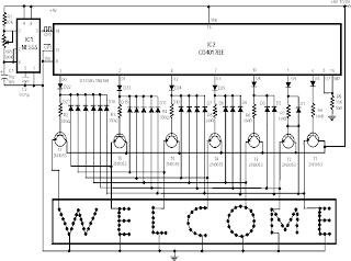
Running Message Display


Light emitting diodes are advan- tageous due to their smaller size, low current consumption and catchy colours they emit. Here is a running message display circuit wherein the letters formed by LED arrangement light up progressively. Once all the letters of the message have been lit up, the circuit gets reset. The circuit is built around Johnson decade counter CD4017BC (IC2). One of the IC CD4017BEs features is its provision of ten fully decoded outputs, making the IC ideal for use in a whole range of sequencing operations.


In the circuit only one of the outputs remains high and the other outputs switch to high state successively on the arrival of each clock pulse. The timer NE555 (IC1) is wired as a 1Hz astable multivibrator which clocks the IC2 for sequencing operations. On reset, output pin 3 goes high and drives transistor T7 to on state. The output of transistor T7 is connected to letter W of the LED word array (all LEDs of letter array are connected in parallel) and thus letter W is illuminated. On arrival of first clock pulse, pin 3 goes low and pin 2 goes high. Transistor T6 conducts and letter E lights up.

Automatic Room Lights


An ordinary automatic room power control circuit has only one light sensor. So when a person enters the room it gets one pulse and the lights come on. When the person goes out it gets another pulse and the lights go off. But what happens when two persons enter the room, one after the other? It gets two pulses and the lights remain in off state. The circuit described here overcomes the above-mentioned problem. It has a small memory which enables it to automatically switch on and switch off the lights in a desired fashion. The circuit uses two LDRs which are placed one after another (separated by a distance of say half a metre) so that they may separately sense a person going into the room or coming out of the room. Outputs of the two LDR sensors, after processing, are used in conjunction with a bicolour LED in such a fashion that when a person gets into the room it emits green light and when a person goes out of the room it emits red light, and vice versa. These outputs are simultaneously applied to two counters. One of the counters will count as +1, +2, +3 etc when persons are getting into the room and the other will count as -1, -2, -3 etc when persons are getting out of the room. These counters make use of Johnson decade counter CD4017 ICs. The next stage comprises two logic ICs which can combine the outputs of the two counters and determine if there is any person still left in the room or not. Since in the circuit LDRs have been used, care should be taken to protect them from ambient light. If desired, one may use readily available IR sensor modules to replace the LDRs. The sensors are installed in such a way that when a person enters or leaves the room, he intercepts the light falling on them sequentially one after the other. When a person enters the room, first he would obstruct the light falling on LDR1, followed by that falling on LDR2. When a person leaves the room it will be the other way round. In the normal case light keeps falling on both the LDRs, and as such their resistance is low (about 5 kilo-ohms). As a result, pin 2 of both timers (IC1 and IC2), which have been configured as monostable flip-flops, are held near the supply voltage (+9V). When the light falling on the LDRs is obstructed, their resistance becomes very high and pin 2 voltages drop to near ground potential, thereby triggering the flip-flops. Capacitors across pin 2 and ground have been added to avoid false triggering due to electrical noise. When a person enters the room, LDR1 is triggered first and it results in triggering of monostable IC1. The short output pulse immediately charges up capacitor C5, forward biasing transistor pair T1-T2. But at this instant the collectors of transistors T1 and T2 are in high impedance state as IC2 pin 3 is at low potential and diode D4 is not conducting. But when the same person passes LDR2, IC2 monostable flip-flop is triggered. Its pin 3 goes high and this potential is coupled to transistor pair T1-T2 via diode D4. As a result transistor pair T1-T2 conducts because capacitor C5 retains the charge for some time as its discharge time is controlled by resistor R5 (and R7 to an extent). Thus green LED portion of bi-colour LED is lit momentarily. The same output is also coupled to IC3 for which it acts as a clock. With entry of each person IC3 output (high state) keeps advancing. At this stage transistor pair T3-T4 cannot conduct because output pin 3 of IC1 is no longer positive as its output pulse duration is quite short and hence transistor collectors are in high impedance state. When persons leave the room, LDR2 is triggered first followed by LDR1. Since the bottom half portion of circuit is identical to top half, this time with the departure of each person red portion of bi-colour LED is lit momentarily and output of IC4 advances in the same fashion as in case of IC3. The outputs of IC3 and those of IC4 (after inversion by inverter gates N1 through N4) are ANDed by AND gates (A1 through A4) are then wire ORed (using diodes D5 through D8). The net effect is that when persons are entering, the output of at least one of the AND gates is high, causing transistor T5 to conduct and energise relay RL1. The bulb connected to the supply via N/O contact of relay RL1 also lights up. When persons are leaving the room, and till all the persons who entered the room have left, the wired OR output continues to remain high, i.e. the bulb continues to remains on, until all persons who entered the room have left. The maximum number of persons that this circuit can handle is limited to four since on receipt of fifth clock pulse the counters are reset. The capacity of the circuit can be easily extended for up to nine persons by removing the connection of pin 1 from reset pin (15) and utilising Q1 to Q9 outputs of CD4017 counters. Additional inverters, AND gates and diodes will, however, be required

Emergency Light


The circuit of automatic emergency light presented here has the following features: 1. When the mains supply (230V AC) is available, it charges a 12V battery up to 13.5V and then the battery is disconnected from the charging section. 2. When the battery discharges up to 10.2V, it is disconnected from the load and the charging process is resumed. 3. If the mains voltage is available and there is darkness in the room, load (bulb or tube) is turned on by taking power from the mains; otherwise the battery is connected to the load. 4. When the battery discharges up to 10.2V and if the mains is not yet available, the battery is completely disconnected from the circuit to avoid its further discharge. The mains supply of 230V AC is stepped down to 18V AC (RMS) using a 230V AC primary to 0-18V AC, 2A secondary transformer (X1), generally used in 36cm B&W TVs. Diodes D1 through D4 form bridge rectifier and capacitor C5 filters the voltage, providing about 25V DC at the output. Charging section includes 33-ohm, 10-watt resistor R2 which limits the charging current to about 425 mA when battery voltage is about 10.2V, or to 325 mA when battery voltage is about 13.5V. When the battery charges to 13.5V (as set by VR2), zener diode D17 goes into breakdown region, thereby triggering triac TR1. Now, since DC is passing through the triac, it remains continuously on even if the gate current is reduced to zero (by disconnecting the gate terminal). Once the battery is fully charged, charging section is cut-off from the battery due to energisation of relay RL2. This relay remains on even if the power fails because of connection to the battery via diode D10. S4, a normally closed switch, is included to manually restart the charging process if required. Battery disconnect and charging restart section comprises an NE555 timer (IC2) wired in monostable mode. When the battery voltage is above 10.2V (as indicated by red LED D15), zener diode (D16) remains in the breakdown region, making the trigger pin 2 of IC2 high, thereby maintaining output pin 3 in low voltage state. Thus, relay RL3 is on and relay RL4 is off. But as soon as the battery voltage falls to about 10.2V (as set by preset VR1), zener diode D16 comes out of conduction, making pin 2 low and pin 3 high to turn on relay RL4 and orange LED D13. This also switches off relay RL3 and LED D15. Now, if the mains is available, charging restarts due to de-energisation of relay RL2 because when relay RL4 is on, it breaks the circuit of relay RL2 and triac TR1. But if the mains supply is not present, both relays RL3 and RL1 de-energise, disconnecting the battery from the remaining circuit. Thus when battery voltage falls to 10.2 volts, its further discharge is eliminated. But as soon as the mains supply resumes, it energises relay RL1, thereby connecting the battery again to the circuit. Light sensor section also makes use of a 555 timer IC in the monostable mode. As long as normal light is falling on LDR1, its resistance is comparatively low. As a result pin 2 of IC3 is held near Vcc and its output at pin 3 is at low level. In darkness, LDR resistance is very high, which causes pin 2 of IC3 to fall to near ground potential and thus trigger it. As a consequence, output pin 3 goes high during the monostable pulse period, forward biasing transistor T3 which goes into saturation, energising relay RL5. With auto/bypass switch S2 off (in auto mode), the load gets connected to supply via switch S3. If desired, the load may be switched during the day-time by flipping switch S2 to on position (manual). Preset VR3 is the sensitivity control used for setting threshold light level at which the load is to be automatically switched on/off. Capacitors with the relays ensure that there is no chattering of the relays. When the mains is present, diode D8 couples the input voltage to regulator IC1 whereas diode D10 feeds the input voltage to it (from battery) in absense of mains supply. Diode D5 connects the load to the power supply section via resistor R5 when mains is available (diode D18 does not conduct). However, when mains power fails, the situation reverses and diode D18 conducts while diode D5 does not conduct. . The load can be any bulb of 12 volts with a maximum current rating of 2 amperes (24 watts). Resistor R5 is supposed to drop approximately 12 volts when the load current flows through it during mains availability . Hence power dissipated in it would almost be equal to the load power. It is therefore desirable to replace R5 with a bulb of similar voltage and wattage as the load so that during mains availability we have more (double) light than when the load is fed from the battery. For setting presets VR1 and VR2, just take out (desolder one end) diodes D7, D10 and D18. Connect a variable source of power supply in place of battery. Set preset VR1 so that battery-high LED D15 is just off at 10.2V of the variable source. Increase the potential of the variable source and observe the shift from LO BAT LED D13 to D15. Now make the voltage of the source 13.5V and set preset VR2 so that relay RL2 just energises. Then decrease the voltage slowly and observe that relay RL2 does not de-energise above 10.2V. At 10.2V, LED D15 should be off and relay RL2 should de-energise while LED D13 should light up. Preset VR3 can be adjusted during evening hours so that the load is on during the desired light conditions

Automatic Dual output Display


This circuit lights up ten bulbs sequentially, first in one direc- tion and then in the opposite direction, thus presenting a nice visual effect. In this circuit, gates N1 and N2 form an oscillator. The output of this oscillator is used as a clock for BCD up/down counter CD4510 (IC2). Depending on the logic state at its pin 10, the counter counts up or down. During count up operation, pin 7 of IC2 outputs an active low pulse on reaching the ninth count. Similarly, during count-down operation, you again get a low-going pulse at pin 7. This terminal count output from pin 7, after inversion by gate N3, is connected to clock pin 14 of decade counter IC3 (CD4017) which is configured here as a toggle flip-flop by returning its Q2 output at pin 4 to reset pin 15. Thus output at pin 3 of IC3 goes to logic 1 and logic 0 state alternately at each terminal count of IC2. Initially, pin 3 (Q0) of IC3 is high and the counter is in count-up state. On reaching ninth count, pin 3 of IC3 goes low and as a result IC2 starts counting down. When the counter reaches 0 count, Q2 output of IC3 momentarily goes high to reset it, thus taking pin 3 to logic 1 state, and the cycle repeats. The BCD output of IC2 is connected to 1-of-10 decoder CD4028 (IC4). During count-up operation of IC2, the outputs of IC4 go logic high sequentially from Q0 to Q9 and thus trigger the triacs and lighting bulbs 1 through 10, one after the other. Thereafter, during count-down operation of IC2, the bulbs light in the reverse order, presenting a wonderful visual effect

Pot plant water tester electronic


This simple device checks if their is water in a pot plant. You stick the two probes(paperclips)into the pot plant and if the LED lights, it means there is water in the pot plant.
You need to adjust the 47k potentiometer to set the level at which the LED goes on.

Programmable Digital Code Lock


A programmable code lock can be used for numerous
applications in which access to an article/gadget is to
be restricted to a limited number of persons. Here is yet
another circuit of a code lock employing mainly the CMOS
ICs and thumbwheel switches (TWS) besides a few other
components. It is rugged and capable of operation on
voltages ranging between 6 and 15 volts. The supply
current drain of CMOS ICs being quite low, the circuit
may be operated even on battery.


The circuit uses two types of thumbwheel switches. switch
numbers TWS1 through TWS8 are decimal-to-BCD converter
type while switch numbers TWS9 through TWS16 are 10-input
multiplexer type in which only one of the ten inputs may
be connected to the output (pole). One thumbwheel switch
of each of the two types is used in combination with IC
CD4028B (BCD to decimal decoder) to provide one digital
output.Eight such identical combinations of thumbwheel
switches and IC CD4028 are used. The eight digital
outputs obtained from these combinations are connected to
the input of 8-input NAND gate CD4068.For getting a logic
high output, say at pole-1, it is essential that decimal
numbers selected by switch pair TWS1 and TWS9 are
identical, as only then the logic high output available
at the Specific output pin of IC1 will get transferred to
pole-1. Accordingly, when the thumbwheel pair of switches
in each combination is individually matched, the outputs
at pole-1 to pole-8 will be logic high.This will cause
output of 8-input NAND gate IC CD4068b to change over
from logic high to logic low, thereby providing a high-
to-low going clock pulse at clock input pin of 7-stage
counter CD4024B, which is used here as a flip-flop (only
Q0 output is used here).The output (Q0) of the flip-flop
is connected to a relay driver circuit consisting of
transistors T1 and T2. The relay will operate when Q0
output of flip-flop goes low. As a result transistor T1
cuts off and T2 gets forward biased to operate the
relay.Switch S1 is provided to enable switching off
(locking) and switching on (unlocking) of the relay as
desired, once the correct code has been set.
With the code set correctly, the NAND gate output will
stay low and flip-flop can be toggled any number of
times, making it possible to switch on or switch off the
relay, as desired. Suppose we are using the system for
switching-on of a deck for which the power supply is
routed via the contacts of the relay. The authorised
person would select correct code which would cause the
supply to become available to the deck. After use he will
operate switch S1 and then shuffle the thumbwheel
switches TWS1 through TWS8 such that none of the switches
produces a correct code. Once the code does not match,
pressing of switch S1 has no effect on the output of the
flip-flop.Switches TWS9 through TWS16 are concealed after
setting the desired code. In place of thumbwheel switches
TWS1 through TWS8 DIP switches can also be used
Service TV,LCD,Plasma,TV Proyektor,DLP Hub: 021.3282.6552

Service LCD TV